SiP Solutions for Sensing & Communications
As demand for higher data throughput grows, companies are increasingly turning to Silicon (Si) photonic integrated circuits (PIC) solutions to reduce cost and port densities. The key enabler is a light source that easily bonds with these Silicon Photonics (SiP) platforms and allows efficient coupling of light.
At DenseLight, we provide Platform Agnostic Laser Solutions which supports both conventional and customer specific packaging technologies using proprietary IP.
Our key enablers are the Integrated Spot-Size-Converter (SSC) and Flip-Chip Capability.
By introducing an Indium Phosphide (InP)-SSC, spot size can be increased 3x, 4x or 5x, and relaxes alignment precision by corresponding 3x, 4x or 5x when flip-chip particular device onto a platform.
Both these technologies are also applying on our product development listed below.
Why Integration Matters:
Packaging and testing are a large fraction of BOM cost of conventional Photonics devices. Integration of devices is the only effective means to
- Improve size, power, cost, speed, reliability and scalability
- Enable new functionalities
- Drive disruption in optical communications
DenseLight’s new generation of InP optoelectronics is designed for flip-chip wafer level hybrid integration on Silicon Photonics and Optical Interposer Platforms.
DenseLight InP-SSC product development program including:
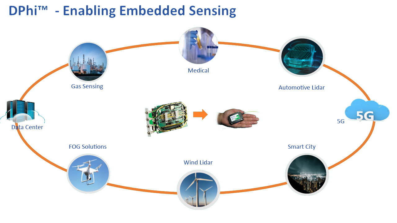
- SLED – for sensing applications
- Waveguide Quad-PIN (100Gbps, 400Gbps)
- DFB laser – CW, CWDM, DML
- Gain chip – 1310nm, 1550nm band
- SOA – 1310nm, 1550nm band
Contact Us
We are ready to lead you into the future of light no matter where your business operates.

